Getting Started
Introduction to System on a Chip (SoC)
Summary
If you have never worked with SoCs, this page will help you understand why an SoC like the DE10-Nano is quite different from a regular FPGA.
SoCs are Different From Standard FPGAs
On a standard Field Programmable Gate Array (FPGA) (Xilinx XC7A100T, Agilex 3 A3CZ135BB18AE7S), all peripherals are connected to various pins on the FPGA. However, on SoCs like that on the DE10-Nano, some peripherals are connected to pins on the FPGA and others are connected to the Hard Processor System (HPS). For example, in the block diagram below, the HDMI controller is connected to pins on the FPGA. To access these pins from the HPS, you need to build a system to wire those pins from the FPGA to a memory addressable region on the FPGA through the FPGA fabric and AXI bus.
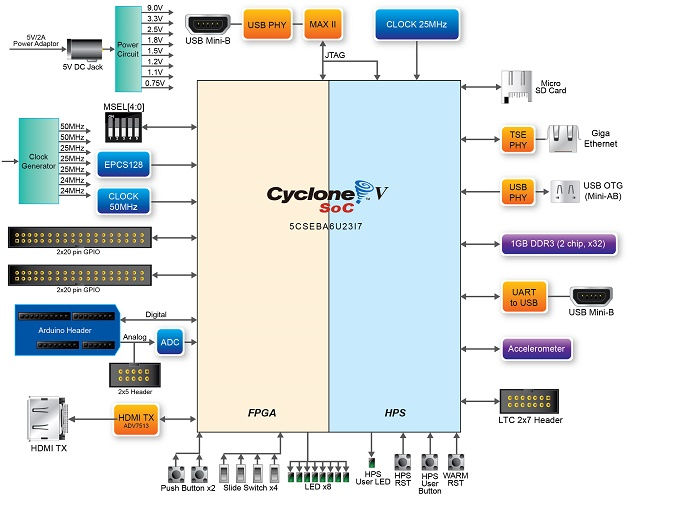
The HPS is etched in silicon and cannot be changed by programming unlike the FPGA, where one can change what the behavior and the logic being run. It is like someone carved out a section of silicon out of the FPGA and dropped an ARM Cortex A9 in and connected it to the FPGA.
I'm comfortable with basic FPGAs, I want to use the HPS, so how?!
When you start trying to learn this, you realize you're now a bit out of the hobbyist domain and are in the professional domain. What this means is:
- Not easy to find documentation.
- Forum responses take days/weeks because the folks are busy with day jobs (Intel community, Rocketboards, reddit)
- Compilation times go through the roof. Not uncommon to have a design build for 10-15 minutes after which you copy it to the SD Card only to find that it doesn't work and you have no idea why. If you are doing this as a hobby, expect that a simple hello world tutorial may take the whole weekend or 2 weekends.
- Version mismatch. The quartus version or the kernel version you have at hand is different from the one in the documentation. Kernel version is easier to fix since you can just get an image that works. But quartus version is harder because of software obsolosence. Maybe you can download Quartus 17.0 and it works, but maybe you can't for the linux distro you are running.
- Software is unbelievably bad. I don't mean this as judgement. It's just a fact. Coming from a software background, you may be used to the polish of intellij, eclipse or cloud platforms. But quartus is nothing like that. It uses cygwin with shell scripts but has windows batch files and bash scripts and oh god! For someone starting out, this was just painful.
- To start using the HPS, I have found it easier to use Linux as the main OS for development. I do this with an Ubuntu 24.04 LTS laptop, but a VM should work.
- You will need the following tools to work with the DE10-Nano:
- Quartus Prime Lite 18.1 (Any newer and you lose the ability to compile Terasic's GHRD)
- ModelSim-Intel FPGA EDition (for testing your designs)
- Cyclone V Device Support
- Intel SoC Embedded Development Suite Standard Edition (Available in standard under additional tools) - This is very important if you want to develop using the HPS as the tools and utilities it provides are needed to work compile and write applications.
How does the HPS interact with the SoC?
Imagine you have an FPGA-only board (like the nandland go) and a processor-only board (like an Arduino or raspberry pi). How would you interface them together if you wanted them to talk to each other? You would use one of the communication standards that both platforms understand so that they can talk to each other such as SPI, I2C, Ethernet, etc. This is usually available in hardware in Raspberry PI and/or Arduino and you don't need to implement them from scratch. However, you need to implement a design on the FPGA which supports one of these protocols and then they can communicate with each other.
On SoCs, they use a similar protocol which is called an Avalon Bus (on Altera) and AXI Bus (on Altera and Xilinx). This bus protocol allows for fast communication between the two. These bus architectures are very complicated that it takes a fair bit of study to learn these. Thankfully, Quartus comes with a tool called Platform Designer (previously called QSYS) which makes it easier to work with this without having to know too much about how the bus works.
Additional Resources
- The DE10-Nano CD-Rom - This is the most important resource as it includes the Golden Hardware Reference Design (GHRD) which is used as the starting point most times. It also includes tools which can be used to generate the starter code. Make sure you download the right revision, there is a doc for this on the Terasic resources page.
- RSYocto - This is an excellent embedded linux distro that has some magical utilities that make programming the FPGA a cakewalk. I've used this and it is partly the inspiration for me to learn more on how to build my own distribution.
- Hello world on DE1-SOC using Platform Designer. This was the eye opener for me and took an entire weekend the first time. Study this slowly and carefully and follow the exact same steps to get an LED working by communicating from the HPS to the FPGA. While it is for the DE1-SOC, the steps are identical to the DE10-Nano. Just copy the values from the GHRD on the CD-ROM instead of the values he uses in the video.
- Building embedded linux for the DE10-Nano - This is another incredible resource that talks about everything end to end including the device tree and building a linux distro. There are many steps which have been used and referenced directly from here.
- Classroom videos on DE1-SoC - These are a series of 25 videos on the DE1-SOC which I found very helpful. I have only gone through the first 3-4 but they are quite interesting. Good if you want an introduction on how you would go about building a design on an SoC.
Introduction to the Terasic DE10-Nano
The Terasic DE10-Nano development board, based on an Intel® SoC FPGA, provides a reconfigurable hardware design platform for makers, IoT developers and educators. Featuring two GPIO expansion headers, an Arduino* header, high-speed DDR3 memory, an HDMI* port and ethernet networking, the board provides a robust and feature rich platform to create many exciting IoT applications.
Developers and makers are invited to discover the performance of a low-power embedded processor integrated with the flexibility of programmable logic. Divided into two distinct parts, the Intel® Cyclone® FPGA SoC device is made of a hard processor system (HPS) and a Field Programmable Gate Array (FPGA). While the HPS is a general purpose processor (based on a dual-core ARM Cortex-A9* processor), the FPGA is a parallel processing engine on which you can create custom hardware to accelerate fixed function algorithms or for extending the I/O capabilities of the device.
Terasic DE10-Nano Kit Contents
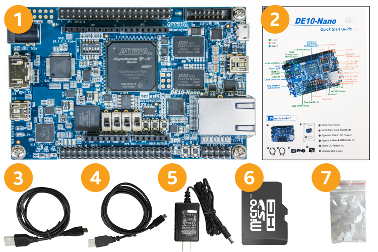
The Terasic DE10-Nano kit should come with 7 items:
- Terasic DE10-Nano Board
- Quick Start Guide
- Type A to Micro-B USB Cable
- Type A to Mini-B USB Cable
- 5V (2A) power supply
- microSD Card
- A bag of 4 silicon foot stands
The Altera Cyclone V SE 5CSEBA6U23I7
The Altera Cyclone V SE 5CSEBA6U23I7 is a high-performance System-on-Chip (SoC) FPGA designed for low-power, cost-sensitive embedded applications. It integrates a dual-core ARM Cortex-A9 MPCore processor with CoreSight, operating at up to 800 MHz, alongside an FPGA fabric featuring 110,000 logic elements (LEs). Built on TSMC’s 28 nm low-power process technology, it offers up to 13.59 Mb of embedded memory through M10K and MLAB blocks, and supports advanced I/O capabilities, including PCIe, USB, and DDR3 memory interfaces. The device is housed in a 672-pin UBGA package (23x23 mm) and provides flexible programmable interconnects for customized designs, making it ideal for applications in digital signal processing, hardware acceleration, and embedded systems requiring robust performance and energy efficiency.